Scanning tunneling microscope
From Wikipedia, the free encyclopedia.
The scanning tunneling microscope (not to be confused with scanning electron microscopes), or STM, was invented in 1981 by Gerd Binnig and Heinrich Rohrer of IBM's Zurich Lab in Zurich, Switzerland. The invention garnered the two a Nobel Prize in Physics in 1986. The STM allows scientists to see and position individual atoms with higher resolution than its related cousin, the atomic force microscope (AFM). Both the STM and the AFM fall under the class of scanning probe microscopy instruments.
It is used to obtain images of conductive surfaces at an atomic scale 2 x 10⁻¹⁰ m or 0.2 nanometre. It can also be used to alter the observed material by manipulating individual atoms, triggering chemical reactions, and creating ions by removing individual electrons from atoms and then reverting them to atoms by replacing the electrons.
The acronym STM is used for both scanning tunneling microscope and scanning tunneling microscopy.
Contents |
Overview
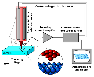
The STM is a non-optical microscope which employs principles of quantum mechanics. An atomically sharp probe (the tip) is moved over the surface of the material under study, and a voltage is applied between probe and the surface. Depending on the voltage electrons will "tunnel" (this is a quantum-mechanical effect) or jump from the tip to the surface (or vice-versa depending on the polarity), resulting in a weak electric current. The size of this current is exponentially dependent on the distance between probe and the surface. Obviously, for a current to occur the substrate being scanned must be conductive. Insulators cannot be scanned through the STM.
A servo loop (feedback loop) keeps the tunneling current constant by adjusting the distance between the tip and the surface (constant current mode). This adjustment is done by placing a voltage on the electrodes of a piezoelectric element. By scanning the tip over the surface and measuring the height (which is directly related to the voltage applied to the piezo element), one can thus reconstruct the surface structure of the material under study. High-quality STMs can reach sufficient resolution to show single atoms. The STM will get within 2nm of what it is observing.
Use of the STM
The scanning tunneling microscope is one of the most important tools for surface physics and surface chemistry, where it shows the structure of the topmost layer of atoms or molecules, e.g., defects and surface domain formation, morphology of thin films grown by various deposition techniques or modifications of surfaces by chemical processes.
For high-resolution of metals and semiconductors, the STM is usually operated in ultrahigh vacuum to avoid contamination or oxidation of the surface. Samples that are less sensitive to the atmosphere, such as graphite, gold, self-assembled monolayers and Langmuir-Blodgett films can be imaged with high resolution under air. The tip of an STM can be also immersed into an electrochemical cell to study processes in electrochemistry (electrochemical STM).
Far from simply a fancy microscope, the STM offers much in the way of surface science studies. Conduction mechanisms can be studied by analyzing a substrate via scanning tunneling spectroscopy, or STS, during which the feedback loop is momentarily interrupted during a scan to obtain dI/dV (point conductance) measurements. It is also possible to take other forms of spectra, such dI/dZ spectra, which is useful in studing the work function (or rather, the vaccuum energy barrier height) of a material. STS also provides information on the density of states of the substrate material. Furthermore, the STM can be used to study charge transport mechanisms in molecules or other extremely small structures such as carbon nanotubes.
STM is also a tool for modification of surfaces through various methods such as indenting the tip or modification of the substrate by the electrons emitted from the tip. At low temperatures (typically, 4 K) it is even possible to move single atoms with high accuracy by carefully "pushing" or "dragging" them with the tip of an STM. Since STM can be used as both a tool and an observation instrument on the nanometer scale it has been vital for the emergence of the nanosciences.
See also
- Microscopy
- Scanning probe microscopy
- Scanning tunneling spectroscopy
- Electrochemical scanning tunneling microscope
- Atomic force microscope
External links


